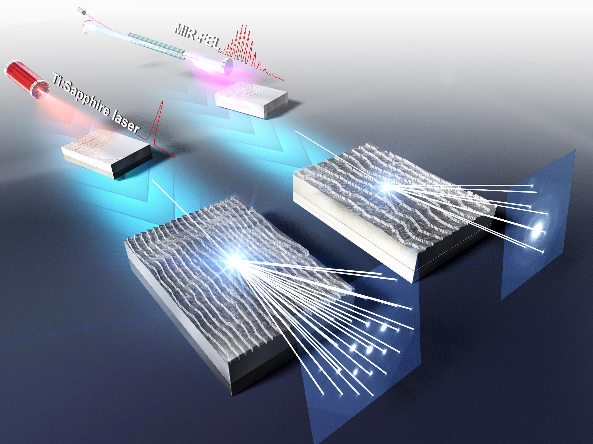

By utilizing a Ti:Sapphire laser and a mid-infrared free-electron laser (MIR-FEL) to construction silicon, scientists have demonstrated how laser-induced periodic floor construction (LIPSS) varies relying on the laser properties. Credit score: Reina Miyagawa of Nagoya Institute of Know-how
Researchers have recognized the results of the selection of laser on LIPSS, offering perception into key manufacturing parameters.
The digital and optical units that we use every day, akin to cell phones, LEDs, and photo voltaic cells use transistors and different constituents which are persistently getting smaller and extra compact. With an ever-growing want for computing energy, storage, and power effectivity, this development will solely proceed to new extremes.
Producing such small parts for digital units requires the machining and preparation of buildings on sub-micron scales, as much as tons of of occasions smaller than the width of a human hair. However present strategies for the nanofabrication of surfaces use photolithography and e-beam lithography— strategies which are sophisticated, extraordinarily costly, usually inaccessible, and require excessive ranges of experience.
Laser-induced periodic floor construction (LIPSS) has been earmarked as a novel and potential various to those strategies. In LIPSS, femtosecond lasers are used to ship ultrashort laser pulses that spontaneously result in the formation of periodic patterns on the floor which are a lot smaller than the laser wavelength.
A well known parameter in LIPSS is the selection of laser wavelength, which instantly impacts the periodicity of the shaped buildings. Nonetheless different parameters have remained unknown. The foremost considerations concerning the standardized use of LIPSS embody the standard of the shaped floor construction, specifically the crystallinity of the substrate, potential for defects, and pressure. To persistently produce LIPSS with controllable properties and traits for particular functions, it’s important to know which laser sources must be used for which explicit want.
Via an applicable selection of laser properties, laser-induced interval floor construction (LIPSS) could be tuned and tailor-made for particular functions by manipulating its defects, pressure, and periodicity. Credit score: Reina Miyagawa of Nagoya Institute of Know-how
To reply these questions in additional depth, a Japanese analysis collaboration led by scientists from the Nagoya Institute of Know-how, has now instantly investigated the assorted parameters which are influenced by laser selection. The work, in collaboration with Osaka College, Tokai College, Kyoto College, and the Japan Atomic Vitality Company (JAEA), was led by Assistant Professor Reina Miyagawa of the Nagoya Institute of Know-how, alongside Affiliate Professor Norimasa Ozaki of Osaka College, and Professor Masaki Hashida of Tokai College, who can also be a researcher at Kyoto College. Their findings have been revealed within the journal Scientific Reports.
“In our study, we chose silicon as a substrate, as it is a material used in many optoelectronic devices the world over, like transistors, mobile phones, and solar cells,” explains Dr. Miyagawa.
The researchers used two different femtosecond lasers on the substrate. In one experiment, a titanium and sapphire (Ti:Sapphire) laser system with pulses of 0.8 µm was used to structure the silicon at energies higher than the band-gap energy. In the other experiment, the researchers used a free-electron laser at mid-infrared pulses of 11.4 µm, which could probe the effect at energies lower than the sample band-gap energy. The analysis of the LIPSS samples was done both microscopically and macroscopically. The microscopic crystallinity and purity were studied using transmission electron microscopy (TEM), while a more macroscopic analysis of the strain and stability of the wider structure was investigated using synchrotron high-energy X-ray diffraction (XRD).
“When the Ti:Sapphire laser was used, the observed LIPSS retained the highly crystalline nature of the silicon but seemed to take on some residual strain. In contrast, the LIPSS which was formed by the mid-infrared free-electron laser led to some clearly visible defects. However, there was no observable strain to the system whatsoever,” adds Dr. Miyagawa.
This study constitutes the first report on the high-resolution, microscopic and macroscopic observations of crystallinity in LIPSS using synchrotron high-energy x-ray diffraction. The findings indicate how LIPSS can be tuned and tailored for specific applications by manipulating its defects, strain, and periodicity, through an appropriate choice of laser. Continued research along these lines can further open the pathway toward the widespread application of LIPSS to achieve the cost-effective, simple, and accessible fabrication of nanostructured surfaces for applications in a wide range of optoelectronic devices.
Reference: “Crystallinity in periodic nanostructure surface on Si substrates induced by near- and mid-infrared femtosecond laser irradiation” by Reina Miyagawa, Daisuke Kamibayashi, Hirotaka Nakamura, Masaki Hashida, Heishun Zen, Toshihiro Somekawa, Takeshi Matsuoka, Hiroyuki Ogura, Daisuke Sagae, Yusuke Seto, Takahisa Shobu, Aki Tominaga, Osamu Eryu and Norimasa Ozaki, 5 December 2022, Scientific Reports.
DOI: 10.1038/s41598-022-25365-1
Supply By https://scitechdaily.com/unlocking-the-secrets-of-laser-induced-periodic-surface-structures-on-silicon/